LASERtrim® Capacitors for RF Circuit Tuning
LASERtrim® capacitors are laser adjustable monolithic ceramic surface mount devices designed for precise functional tuning of RF circuits.
With superior reliability compared to conventional multi-layer chip capacitors, LASERtrim® capacitors eliminate concerns such as capacitance drift and flux entrapment associated with mechanical trimmers.
Features:
- Superior Performance: Excellent post-trim Q and ESR at 100 - 2000 MHz
- High Reliability: No capacitance drift or flux entrapment
- Versatile Sizes: Available in 0603 to 1210 chip sizes
- Efficient Packaging: Nickel barrier terminations, tape and reel packaging
- Compatibility: Perfect for high volume SMT auto-placement and reflow techniques
- High Accuracy Tuning
- Automates Functional Tuning
- Small, Standard SMD Chip Sizes
- Lower Placement Cost vs Mechanical Solutions
- Highly Stable and Reliable After Adjustment
- RoHS Compliant Parts Available
LASERtrim® capacitors are the top choice for oscillator, filter, and antenna circuit tuning in various wireless RF products. Enhance your RF circuit design with these high-quality, drift-free capacitors.
Applications:
- Mobile Phones
- Wireless LAN
- Cable Modems
- RFID
- Wireless Transceivers
- Custom Applications
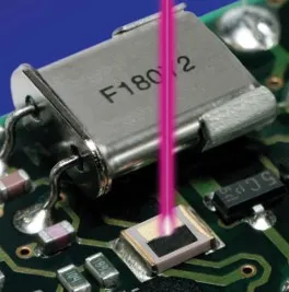
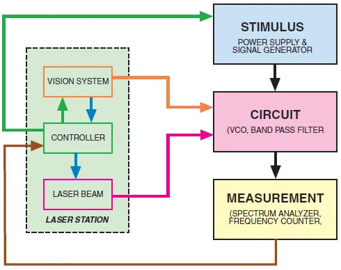
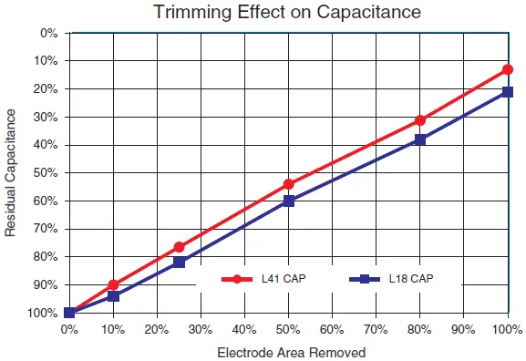
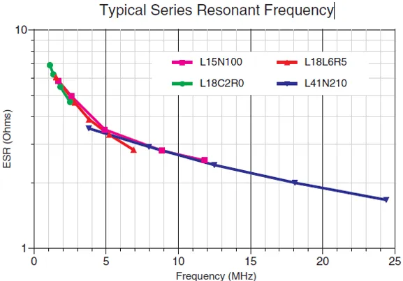
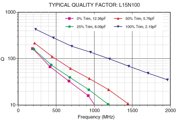
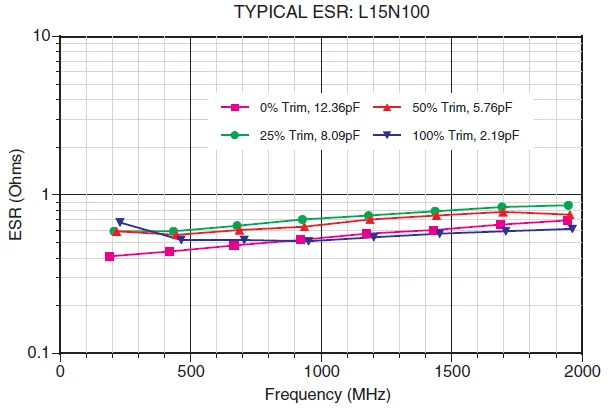
LASERtrim® tuning capacitors are used to provide functional RF circuitry tuning. The tuning is normally performed at a laser station integrated into the automated assembly line at a point beyond any operations that may significantly alter the circuit’s RF characteristics. Tuning is performed by a computer controlled YAG laser beam which removes or “trims” the top electrode material of the LASERtrim® thereby decreasing it’s capacitance. Circuit parameters such as frequency or voltage are monitored during tuning and fed back to the laser controller achieving extremely precise results. Typical capacitance change in relation to the amount of electrode removal is shown in the graphs below.
| Working Voltage: | 50 Volts DC |
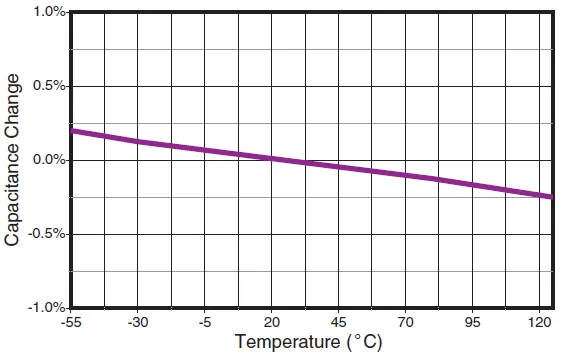
| Temperature Coefficient: | 0 ± 30ppm /°C, -55 to 125°C |
| Dissipation Factor: | 0.0015 (0.15%) max, 25°C |
| Insulation Resistance: | > 10 GΩ @ 25°C, WVDC; 125°C IR is 10% of 25°C rating. |
| Dielectric Strength: | 2.5 X WVDC, 25°C, 50mA max |
| Test Perameters: | 1 MHz ±50kHz, 1.0±0.2 VRMS, 25°C |
| Environmental: | Meets the mechanical & environmental characteristics as given for the JTI S-Series capacitors (see second page of the S-Series specification sheet), except terminal adhesion for all sizes is > 2.0 lbs. |
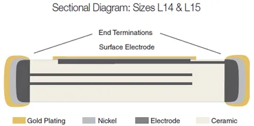
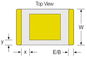
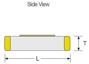
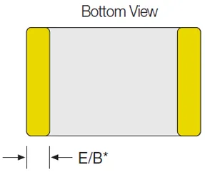
| Size | L14 (EIA 0603) | L15 (EIA 0805) | L41 (EIA 1210) |
|---|---|---|---|
| inches | (mm) | inches | |
| L | .058 ±.008 | (1.47 ±.20) | .080 ±.008 |
| W | .032 ±.008 | (0.81 ±.20) | .050 ±.008 |
| T | .025 MAX | (0.64 MAX) | .025 ±.005 |
| x & y | .004 MIN | (0.10 MIN) | .004 MIN |
| E/B | .005 MAX | (0.13 MAX) | .005 MIN |
| E/B* | .012 MAX | (0.30 MAX) | N/A (L14 Only) |
Soldering Profiles and Guidelines for SMT Ceramic Components
General
Ceramic chip capacitors exhibit excellent reliability characteristics providing that proper circuit design techniques and controlled assembly processes are utilized. Due to the ceramic capacitor’s crystalline micro-structure these components are susceptible when exposed to excessive thermal or mechanical shock during circuit processing. It should be noted that micro-cracks in ceramic can be difficult to detect with normal post assembly visual and electrical testing and can pose a significant threat to reliable field operation. For this reason it is recommended that the assembly qualification process employ suitable testing to expose the presence of micro-cracking conditions.
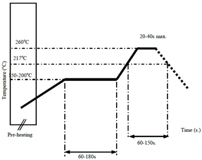
Figure 1: Solder Reflow Profile for Ceramic Capacitors and Inductors (JEDEC J-STD-020C compatible)
Ceramic components’ leads composition and soldering compatibility
High Frequency Ceramic Capacitors & Inductors - Offered with standard tin plated nickel-barrier terminations compatible with solder flow and reflow processes.
Single Layer Capacitors - Offered with Titanium-Tungsten/Gold and Titanium-Tungsten/ Nickel/Gold thin-film termination as well as legacy Platinum/Palladium/Gold terminations.
LASERtrim® Capacitors - Offered with gold flashed nickel-barrier terminations only. Due to the unique internal construction of the LASERtrim® it is recommended that a conservative reflow temperature profile be used (Fig. 5). Wave soldering is discouraged.
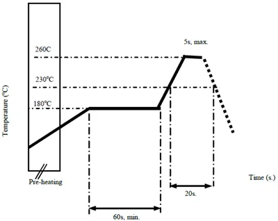
Figure 2: Solder Flow Profile for Ceramic Capacitors and Inductors.
Soldering Iron
Ceramic capacitor attachment with a soldering iron is discouraged due to the inherent limitations on precisely controlling soldering temperature, heat transfer rate, and time. In the event that a soldering iron must be employed the following precautions are recommended.
- Preheat circuit and ceramic component to 150°C
- ever contact the ceramic surface with the iron tip
- 30 watt iron output (max)
- 280°C tip temperature (max)
- 3.0 mm tip diameter (max)
- Limit soldering time to 5 sec.
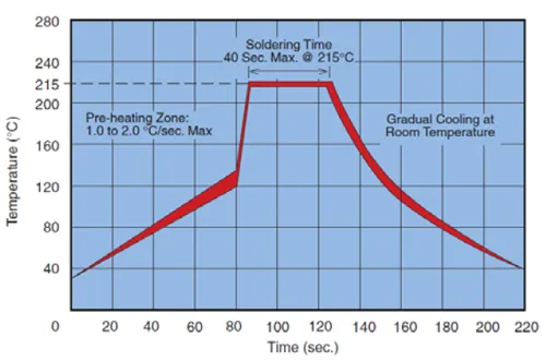
Figure 3: Vapor Phase Profile for MLCCs
Solder Pre-Heat Cycle
Proper preheating is essential to prevent thermal shock cracking of the capacitor. The circuit assembly should be preheated as shown in the recommended profiles at a rate of 1.0 to 2.0°C per second to within 65 to 100°C of the maximum soldering temperature.
- Preheat circuit and ceramic component to 150°C
- ever contact the ceramic surface with the iron tip
- 30 watt iron output (max)
- 280°C tip temperature (max)
- 3.0 mm tip diameter (max)
- Limit soldering time to 5 sec.
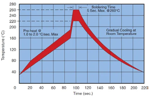
Figure 4: Wave Solder Profile for MLCCs
SMT Soldering Temperatures
Solders typically utilized in SMT have melting points between 179°C and 188°C. Activation of rosin fluxes occurs at about 200°C. Based on these facts a minimum peak reflow temperature of 205°C to 210°C should be established. A maximum peak reflow temperature of 225°C should be adequate in most circumstances. Many reflow process profiles have peaks ranging from 240°C to 260°C and while ceramic capacitors and inductors can withstand soldering temperatures in this range for short durations they should be minimized or avoided whenever possible. Use of PCB mounted multiple thermocouple M.O.L.E. profiling is advised for accurate characterization of circuit heat absorption and maximum temperature conditions.
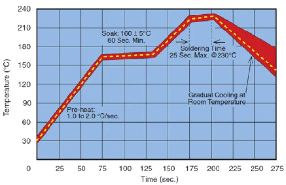
Figure 5: Solder Reflow Profile for LASERtrims®
Reflow Solder
The general term “reflow” refers to several methods used in heating the circuit so that solder paste reflows, or “wetting” of the ceramic capacitor and PCB contacts occurs. These methods include infrared, convection and radiant heating. The size of the solder fillet may be controlled by varying the amount of solder paste that is screened onto the circuit. Recommended temperature limits and times for solder reflow are shown in Figure 1 and 2 for Ceramic Capacitors and inductors and for LASERtrim® in Figure 5.
Vapor Phase
A typical vapor phase soldering process consists of several temperature zones created by saturated vapor from a boiling liquid. As the circuit passes through the zone the vapor condenses on the solder paste, pad, and termination resulting in heat transfer and reflow of the solder paste. Vapor phase reflow produces consistent circuit heating with reflow occurring at a relatively lower temperature that is determined by the known boiling point of the liquid used, typically 215°C. Recommended temperature limits for vapor phase reflow are shown in Figure 3.
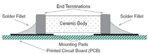
Figure 6
Solder Wave
Wave soldering is perhaps the most rigorous of surface mount soldering processes due to the steep rise in temperature seen by the circuit as it is immersed in the molten solder wave, typically at 240°C. Recommended temperature limits for wave soldering are shown in Fig. 4.
Cool Down Cycle
After the solder reflows properly the assembly should be allowed to cool gradually at room ambient conditions. Attempts to speed this cooling process or immediate exposure of the circuit to cold cleaning solutions may result in thermal shock cracking of the ceramic capacitor.
Solder Fillets
To avoid detrimental effects of thermal and mechanical stress it is essential that the solder fillet be limited to 2/3rds of the overall height of the MLC termination as illustrated in the figure below. The solder fillet can be controlled by solder paste deposition and pad design in reflow and vapor phase processes and by pad design and use of hot air knives in the wave process. As shown in Figure 6.
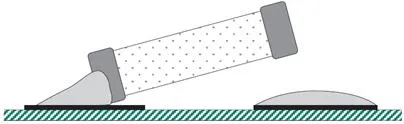
Tomb Stoning/Chip Movement
Tomb-stoning or draw bridging is illustrated in the figure below. Tomb-stoning or other undesirable chip movements may result if unequal surface tension forces exist as the molten solder wets the MLC terminations and mounting pads. This tendency can be minimized by insuring that all factors at both solder joints are equal, namely; pad size, solder mass, termination size, component position and heating. Tomb-stoning is easily avoided through proper design, material selection and proofing of the process. As shown in figure 7.
| Global P/N | Legacy P/N | Size (EIA) | Initial | Tuning Range | 200 MHz | 900 MHz |
|---|---|---|---|---|---|---|
| LTCP500G100R1GG001T | 500L14N100XG4 | 0603 | 10.0 pF | 10.0 - 2.00 pF | > 125 | --- |
| LTCP500G120R1GG001T | 500L14N120XG4 | 0603 | 12.0 pF | 12.0 - 2.00 pF | > 125 | --- |
| LTCT500G100R1GG001T | 500L15N100XG4 | 0805 | 10.0 pF | 10.0 - 1.20 pF | > 75 | --- |
| LTCT500G200R1GG001T | 500L15N200XG4 | 0805 | 20.0 pF | 20.0 - 1.50 pF | > 50 | --- |
| LTDF500G210R1GG001T | 500L41N210XG4 | 1210 | 21.0 pF | 21.0 - 3.00 pF | > 75 | --- |