Thin Film Patterned Substrates
This is Johanson's custom thin film substrates and components design guide. A step-by-step substrate selection, material properties, metal selection, quality standards, design submission and inspection methods.
Features:
- Quick turn prototype to high volume production
- Advanced thin film manufacturing capabilities / features
- Wide array of ceramic substrate materials / metal systems
- Unique customer solutions
- The ability to reduce circuit size and parts count
Substrate Selection
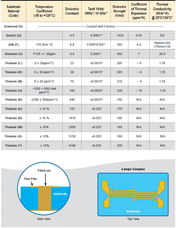
Choosing the correct substrate influences the mechanical and electrical function of a design. Johanson offers a wide range of dielectrics for use in application specific environments. These materials are available in lapped, polished, and “as fired” conditions. These substrates can be metallized or nonmetallized. Metallized substrates may be patterned to customer specifications by chemical etching, abrasive etching, and patterned plating.
Coefficient of thermal expansion (CTE) and thermal conductivity are important parameters for circuits involved with high power. Care should be used when choosing a substrate because differences in CTE values of close metals, like housings or heat-sinks, will cause mismatch stresses in an assembly during temperature changes. Thermal conductivity defines the rate of heat transfer between hot and cold regions of your design. In applications where heat conduction is critical, designers must consider thermal conductivity of available substrates or use filled-vias as an alternative thermal path within a design.
Table 1: Material Electrical and Mechanical Properties
Note: When metallization is requested on both top and bottom sides, the metallization will wrap around the sides as a standard unless otherwise specified.
Johanson Technology offers several different metal schemes to meet customer needs. We offer single-sided or double-sided metallization. Each side can have unique design requirements and metallization. Each metal layer typically has a specific use, whether that be adhesion, barrier or conductor layers. Selection of a metal should be based on electrical functioning demands and/or requirements.
Some designs require pads suitable for solder attachment while others require metals that could readily be wire bonded. Solderable metallization schemes are available by adding Ni or Cu barrier for thin film designs. For optimal wire bond integrity, Johanson recommends a minimum of 100µ” thickness on thin film designs, although good performance can be achieved with as low as 80µ”.
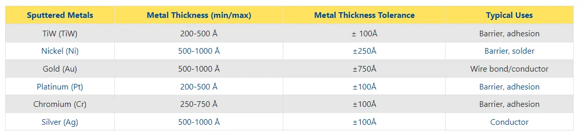
Careful selection of particular metallizations are dependent on requirements for solderability, temperature resistance, wire bonding, and electrical performance. Note: Johanson has capability to sputter and plate other metals not listed in Table 3. We will review special requests for metallizations not listed here.
Table 3: Available Plated Metals
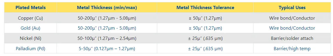
Table 4: Available Sputtered Metals
Precise management of critical geometric features lead to excellent and dependable performances in RF, microwave, and millimeter wave designs. With accurate conductor line widths and spacing, designers can control the characteristic impedance of transmission lines, coupling between RF traces, and even manage thermal loads within RF circuits. Using high quality conductor traces with little variation allows designers to have consistent performance in RF components such as filters and couplers.
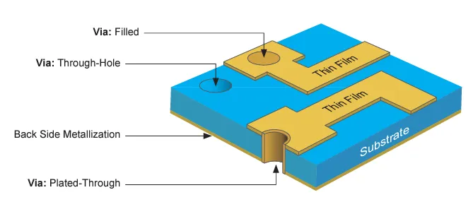
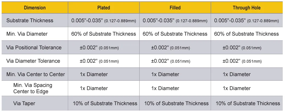
Johanson has advanced experience incorporating vias into substrate designs with demanding requirements. Vias can be offered as either filled, through-hole or plated-through. Engineers must review the existing electrical and thermal properties of their design before deciding between filled or plated-through vias. The overall process is completed by lasering through a substrate from the top to bottom layer and then sputtering or plating over the substrate via opening. Both via options are effective in routing electrical signals from one side to another.
Plated-through vias are often recommended for low-power applications or in designs that require an opening to be maintained. In contrast, filled-vias are best used in high power applications or to enhance thermal properties of the hybrid design. Filled-vias are useful in keeping heat away from the substrate, which in turn helps to prevent defects or circuit failures. Filled-vias offer the lowest RF inductance and thermal resistance. Laser machined vias have a taper equal to approximately 10% of the material thickness.
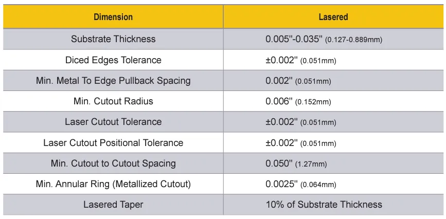
Laser machining is available to provide designers with controlled hole locations, custom shapes and sizes, and superb edge accuracy. Johanson’s team allows engineers to realize flexible designs within the ceramic substrates. Johanson’s standard laser features and tolerances can be visualized below.
We encourage all design engineers to submit their drawings or ideas for quick and easy feedback.
Before submitting your design, use the preferred practices checklist:
- Follow Johanson’s design guidelines and standard specifications
- Provide CAD data in multiple layers
- Identify “A” side and “B” side for double-patterned circuits
- Provide tolerances and annotation
- DWG, DXF, Gerbers, and STEP files are preferred
Information needed:
- Substrate: Material, surface finish, thickness, and dimensions
- Metallizations: Thickness and tolerances
- Conductor traces: Type, spacing, and tolerances
- Other: Inspection or acceptance criteria
| Attribute | Definition of Visual Attribute | Diagram | Acceptable Conditions |
|---|---|---|---|
| Blister | Formation of small to large, broken, or unbroken bubbles | 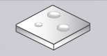 |
Smooth no blisters. |
| Bumps, Fins, and Ridges | Streak of excess material. | 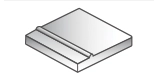 |
Smooth no bumps, fins, or ridges. |
| Burrs | A raised edge or fragment of external material on the surface. | 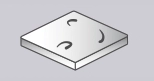 |
Height less than 1 millimeters and diameter less than 10 millimeters. |
| Chips | Visual evidence remaining on the substrate indicative of material loss from corners or edges due to mechanical damage, lack of material integrity, or both. | 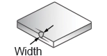 |
Less than 10 millimeters. |
| Cracks | Line on the surface which has split without breaking apart. | 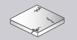 |
Solid no cracks. |
| Pits, Holes, and Pocks | A cavity or void. | 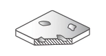 |
Diameter less than 5 millimeters. |
| Scratches | A long, thin, or small gash/cut on the plane. | 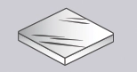 |
Less than 2 millimeters deep and less than 25 millimeters length. |
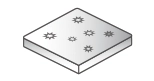
| Snowflakes | Microscopic metallic residue on X-dielectric surfaces. |
|
Smooth no bumps, fins, or ridges. |
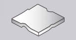
| Warpage | Substrate deformed or misshapen |
|
Height variation less than 10 millimeters per 100 millimeters in length. |
Commitments and Certifications We are committed to making products of the highest quality, performance, and value. Our new design and manufacturing facility employs state of the art equipment and practices. All employees participate in quality awareness and SPC training classes, and our quality system is certified to ISO 9001.
RoHS Standard parts supplied by Johanson Technology, Inc. are fully compliant to the European Union Directives 2002/95/EC, 2011/65/EU, and Annex II (EU) 2015/863 of the European Parliament and of the Council of 31 March 2015 on the Restriction of the use of certain Hazardous Substances in electrical and electronics equipment (RoHS Directives).
REACH Parts (articles) supplied by Johanson Technology meet the requirements for REACH and do not contain any of the SVHC chemicals listed above the levels mandated by the ECHA.
Johanson Technology has made every effort to present data that represents the actual performance of the part.
Johanson Technology reserves the right to make design changes without notice.