Chip Antenna Design Assistance, Tuning, and Characterization Services
Step1: 2 complimentary RF layout reviews of your PCB by a Johanson Technology (JTI) engineer before fabrication to ensure optimum radiated performance. Our engineering team will produce pre-fab board layout (antenna footprint) suggestions, antenna selection, location, and grounding recommendations.
We have available state-of-the-art anechoic test chambers for radiation pattern characterization based on measured data on the client’s PCB.
Refer to:
If appropriate, an NDA agreement can be put in place to facilitate close and detailed technical communication.
Step 2: Once the layout review and prototype manufacturing has occurred, the only requirement is that the client send us a fully populated PCB: all SMDs including batteries (if applicable), connectors, and encasements (they affect RF resonance) mounted and installed. The customer can leave the antenna (optional) and antenna matching components’ slots empty as we will be mounting/soldering them ourselves. The system does not need to be functional; we feed our own passive 0dBm signal directly into the antenna1 for proper isotropic radiation measurements.
• Johanson will test the SMD antenna2 on the original, modified, or optimized PCBThen tune to proper, centered and optimum resonance using appropriately selected Hi-Q Johanson-made inductors and capacitors
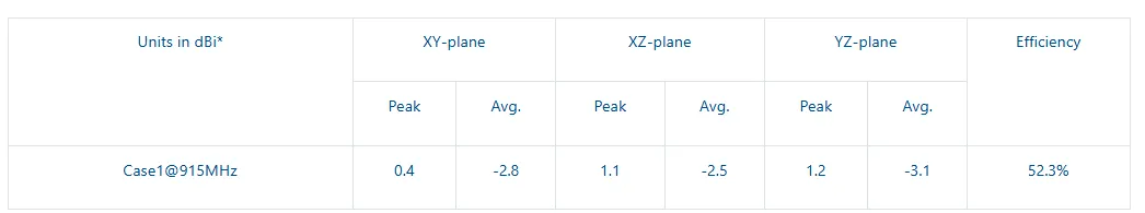
- Measure the radiated performance in an anechoic chamber and provide a 3D plot representing it.
- Client is then sent copies of the new matching circuit schematic with their corresponding values and p/n’s, measured radiated data, and patterns with their corresponding radiated efficiency and gain figures on your PCB. Sometimes this process may require JTI to modify your board in their lab, and to add probes through your enclosure/housing.
- Assemblies may be returned to customer at their request.
The shipping address for the prototypes to be tuned/characterized is:
Johanson Technology, IncAttention: (Responsible Engineer in charge of your case)4001 Calle TecateCamarillo, CA 93012USA
The ultimate goal is to optimize the “Over The Air” performance of your design using Johanson’s extensive design knowledge and application optimization expertise for market success, this entire process takes 2-3weeks, depending on the complexity of the design and environment.
915MHz Chip Antenna tuning and characterization service example:
1 We perform passive measurements only, these are not emission compliance tests
2 This service is only available for JTI antennas