Chip Antenna Layout Considerations for BLE, 802.11, and 2.4G Zigbee
Chip Antenna matching and radiation pattern performance can be dramatically affected by the design/layout of a circuit. Antenna mounting, the antenna's position relative to circuit mismatches, the antenna position relative to adjacent components and ground planes all can affect antenna performance. Thus design engineers must use care when creating a circuit layout which includes an antenna. Johanson Technology chip antenna performance specifications are based on the chip antenna when mounted onto the associated Johanson evaluation board. These evaluation boards serve as a good starting point for designers.
Johanson Technology offers many different chip antennas that operate between 1.5GHz and 6 GHz. To view a complete list of Johanson Technology antennas with links to detailed specifications click here.
Because of the effect of these subtleties, antennas mounted in a specific application are likely to exhibit performance that is different from the published specification. The matching components shown on the test board provide a good starting point for determining the necessary components in a given application. Be sure to keep the antenna free from surrounding ground plane(s), as it is not designed to work against a ground plane or with one in its immediate proximity. Failure to follow this guideline could significantly alter the radiation pattern characteristics.
When determining the matching components needed in an individual application, begin by measuring the return loss (S11) into the matching component(s) feeding the antenna in the same configuration that is planned for the final circuit. Vary the value of the matching components until the return loss dip is centered on the specified operating band.
Some design guidelines are:
- The microstripline feeding the antenna is to be considered part of the antenna resonance system.
- Connect the edge portion of ground planes (the ground plane surrounding the microstripline feeding the antenna to the bottom ground plane layer) with many through holes (vias). These through holes minimize the electric fields which are generated at the edge, minimizing the effects on the antenna performance.
- The length of the microstripline feeding the antenna, and the length and width of the ground plane surrounding that microstripline, together will determine whether the system (antenna, matching and ground plane) acts like a dipole or a monopole. If the ground is about 3-4 cm long and about 1-2 cm wide, then the system will act as a dipole system. If the ground area is large enough, the system will operate like a monopole antenna.
- For best results, the chip antenna needs to be removed from surrounding ground planes by at least the amount shown by the following (assuming horizontal mounting as shown on pages 3 & 4 of this application note)
- More than 2 mm from the shorter edges of the antenna, when mounted as shown on page 3. More than 1 mm from the shorter end of the antenna that is closest to the ground plane, when mounted as shown on page 4.
- More than 4 mm from the longer edge of the antenna (the antenna is mounted on the edge of a PCB, so there is no ground plane adjacent to one of the longer sides) The performance greatly deteriorates if the dimensions are less than the minimum dimensions mentioned above in 4.a and 4.b although the antenna still works.
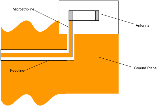
- The feedline that feeds the microstripline (whether coaxial or stripline) should be perpendicular to the microstripline to prevent it from becoming part of the resonance system. (If a feeder becomes an antenna, it leads to deterioration of the desired performance). See the below figure for a figure of this arrangement.
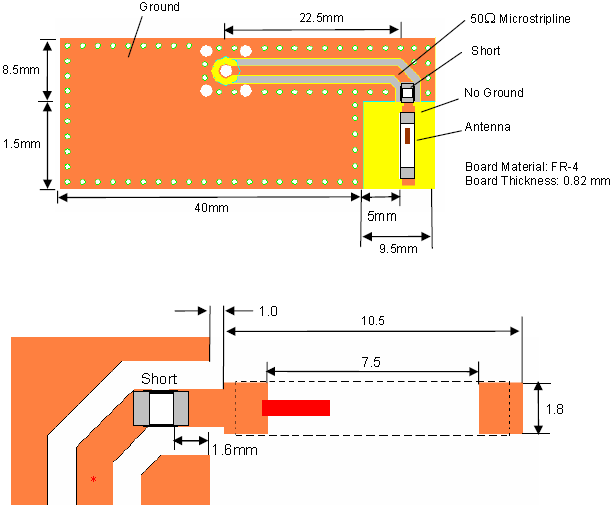
The following is an example of the Johanson Technology 2450AT45A100 Chip Antenna:
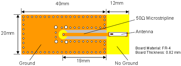
TYPICAL HORIZONTAL ORIENTATION ROUTING
For the antenna to resonate at 2.45 GHz when mounted as shown here, the in-line matching component of 1.2 pF is required.
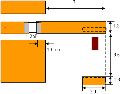
The matching component may be slightly different than that shown depending on distance to ground plane, dielectric constant of PCB, and PCB material thickness.
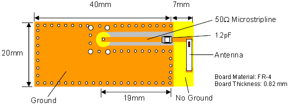
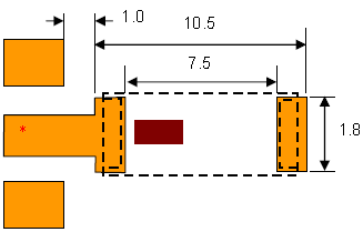
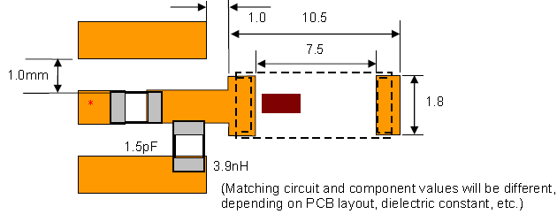
TYPICAL HORIZONTAL ORIENTATION ROUTING (ALTERNATE)
(Matching circuit and component values will be different, depending on PCB layout) *Line width should be designed to match 50. characteristic impedance, depending on PCB material and thickness.
TYPICAL VERTICAL ORIENTATION ROUTING
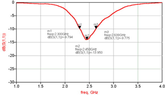
(a) Without Matching Circuits (Moderate Bandwidth)
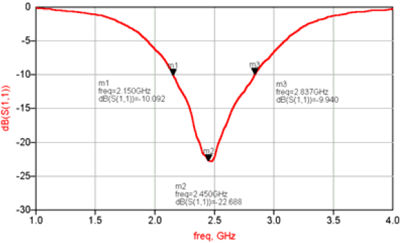
(b) With Matching Circuits (Wide Bandwidth)
*Line width should be designed to match 50. characteristic impedance, depending on PCB material and thickness.
(a) Return Loss Without Matching Circuits
(b) Return Loss With Matching Circuits
Listed here are the matching components needed for other common JTI antennas when mounted on JTI test boards:
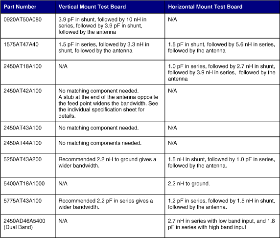
The matching circuit and the component values will be different in every application, depending on PCB material, thickness, etc. The given values are for the JTI test boards, and are good starting values for finding the optimum values for an individual application.