PCB Pad Layout Recommendations
Pad Design & Board Layout Recommendations for Chip Capacitors and Inductors
Solder pad design, solder application, and component placement are important elements of the soldering process. Excessive transfer of thermal or mechanical stresses to the MLC can result from oversized solder fillets.
Nominal pad designs for solder reflow process are listed in Table 1. These guidelines represent a starting point in Printed Circuit Board (PCB) design.
Further information is the Institute for Interconnecting and Packaging Electronic Circuits (ww.ipc.org) has developed and published IPC-SM-782A “Surface Mount Design and Land Pattern Standard”.
High-Q Capacitors
S-Series
G-Series
L-Series
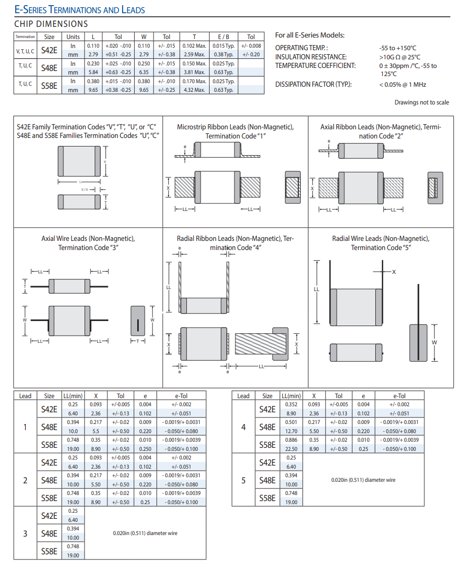
E-Series
Inductors
Wirewound
Ceramic
Lasertrim
Lasertrim
Chipset Specific RF Front-End Chips
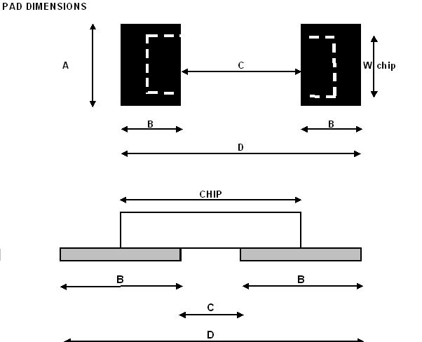
Table 1: Pad Dimensions in inches (mm)
| JTI Ref Capacitors |
JTI Ref Inductors |
EIA Chip Size |
A | B | C | D | ||||
|---|---|---|---|---|---|---|---|---|---|---|
| Min | Max | Min | Max | Min | Max | Min | Max | |||
| R05 | L-05 | 0201 | 0.013 (0.33) |
0.016 (0.41) |
0.008 (0.20) |
0.014 (0.36) |
0.008 (0.20) |
0.014 (0.36) |
0.024 (0.61) |
0.040 (1.02) |
| R07 | L-07 | 0402 | 0.018 (0.46) |
0.024 (0.61) |
0.014 (0.36) |
0.018 (0.46) |
0.012 (0.30) |
0.020 (0.51) |
0.040 (1.02) |
0.056 (1.42) |
| R14 | L-14 | 0603 | 0.028 (0.71) |
0.043 (1.09) |
0.024 (0.61) |
0.028 (0.71) |
0.024 (0.61) |
0.031 (0.79) |
0.072 (1.83) |
0.087 (2.21) |
| R15 | L-15 | 0805 | 0.044 (1.12) |
0.060 (1.52) |
0.024 (0.61) |
0.028 (0.71) |
0.039 (0.99) |
0.047 (1.19) |
0.087 (2.21) |
0.103 (2.62) |
| S42 | N/A | 1111 | 0.130 (3.30) |
0.150 (3.81) |
0.050 (1.27) |
0.060 (1.52) |
0.075 (1.91) |
0.090 (2.29) |
0.175 (4.45) |
0.210 (5.33) |
| S48 | N/A | 2525 | 0.280 (7.11) |
0.300 (7.62) |
0.050 (1.27) |
0.060 (1.52) |
0.200 (5.08) |
0.024 (0.61) |
0.300 (7.62) |
0.360 (9.14) |
| S58 | N/A | 3838 | 0.405 (10.29) |
0.050 (11.43) |
0.050 (1.27) |
0.060 (1.52) |
0.325 (8.26) |
0.370 (9.40) |
0.425 (10.80) |
0.490 (12.45) |
Note: For Single Layer Capacitors (Standard, GBBL), land patterns are unique to each customer design – thus Johanson does not make recommendations for SLC land patterns.
Note: Dimensions given for S48 and S58 case sizes are for reference only. Chips larger than 2225 soldered directly onto a PCB substrate might have a risk of creating thermal and mechanical stress which could results mechanical cracks. As an alternative, JTI recommends using components equipped with ribbons instead.
Solder Fillets
To avoid detrimental effects of thermal and mechanical stress it is essential that the solder fillet be limited to 2/3rds of the overall height of the MLC termination as illustrated in the figure below. The solder fillet can be controlled by solder paste deposition and pad design in reflow and vapor phase processes and by pad design and use of hot air knives in the wave process. As shown in Figure 6
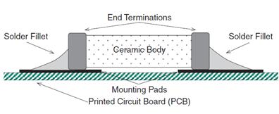
Figure 6
Tomb Stoning/Chip Movement
Tomb-stoning or draw bridging is illustrated in the figure below. Tomb-stoning or other undesirable chip movements may result if unequal surface tension forces exist as the molten solder wets the MLC terminations and mounting pads. This tendency can be minimized by insuring that all factors at both solder joints are equal, namely; pad size, solder mass, termination size, component position and heating. Tomb-stoning is easily avoided through proper design, material selection and proofing of the process. As shown in figure 7
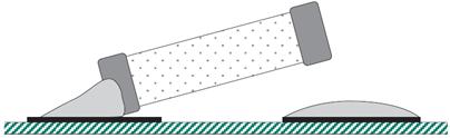
Figure 7